Eagle | PSpice
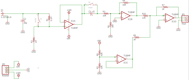
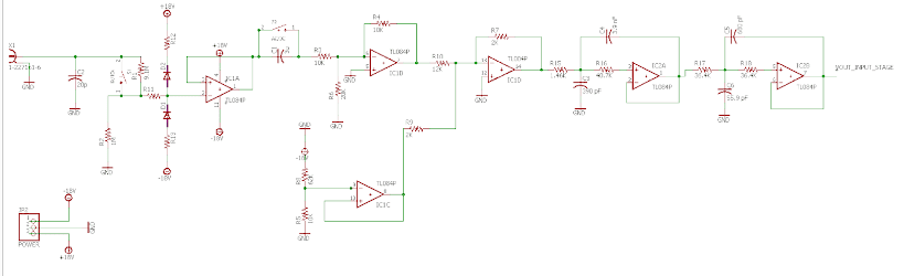
Full schematic of final candidate design, currently at 1x and DC mode
The goal of this project is to design an oscilloscope that meets the functions and specifications given in the assignment handout [1]. The following building blocks and circuit elements could be used: voltage divider to multiply and divide voltages, operational amplifiers to transform voltages, and buffers to remove issues with the loading problem. Each building block’s limitations and weaknesses will be discussed in the following sections.
Design #2 utilizes two fewer op-amps and performs the voltage transformation more efficiently than Design #1. Having fewer op-amps could also reduce the risk of the clipping effect. Thus, Design #2 will become the final design. However, for the AC/DC coupling, there is a tradeoff to the capacitor value; having a high capacitor value prevents attenuation of lower frequency signals, but requires a longer settling time when switching between DC/AC modes. On the other hand, having a low capacitor value requires a low settling time, but may attenuate lower frequency signals. Thus, for the final candidate design, the capacitor will be optimized.
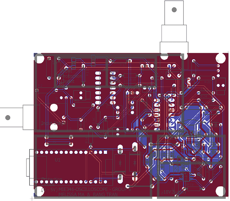
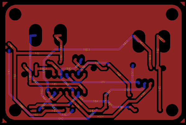
PCB generated in Eagle (Two layers with component and solder)
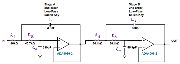
Low Pass Filter Schematic
For the Arduino Nano ADC to properly perform analog to digital conversion, high frequency components of the measured signal needs to be removed. To do so, we utlitized a 2 stage low pass filter. It has a gain of 0db. After optimization, we achieved a -1dB attenuation at 20 KHz, and -32.1 dB attenuation at 50 kHz. This filter fulfills the function by attenuating frequencies up to and including 20 KHz as little as possible (-1dB), and it achieves at least -20 dB at 50 kHz (-32.1 dB).
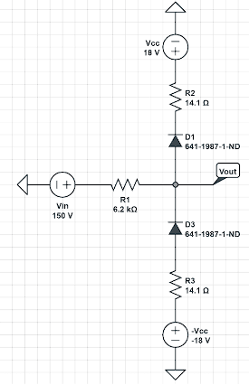
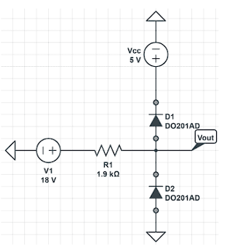
In the case that the oscilloscope user inputs a signal outside the designed signal range of Vin= -15 to 15 V, we aim to design a protection circuit so that the input op-amp of the oscilloscope circuit is unharmed. However, if there is normal operation with no overload, this circuit will not affect the incoming signal.
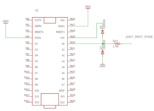
To protect the ADC input on the Arduino Nano from overvoltage, we need to design a ADC protection circuit. To do so, we will make use of the following circuit:
Our topology choice is the boost and inverting combination. This option allows the the user to power the oscilloscope using only one adapter, which simplifies the user experience and reduces the overall cost of the setup. Additionally, by first focusing on creating a +18V output and then inverting it to obtain -18V, the design becomes more modular. This makes it easier to troubleshoot and maintain the circuit, as each part of the design can be tested and improved independently. This advantage also extends to scalability; if the input voltage range needs to be expanded in the future, it would be easier to adjust the design in Option 2 than in Option 1. By using a boost converter, you can accommodate a wider range of input voltages without significantly changing the circuit design. In summary, Option 2 is the recommended choice because it requires only one adapter, offers a modular design, and provides better scalability for future updates. By implementing a boost converter to generate +18V and then using an inverting converter to produce -18V, you can create a power supply that meets the required specifications and offers a better user experience.
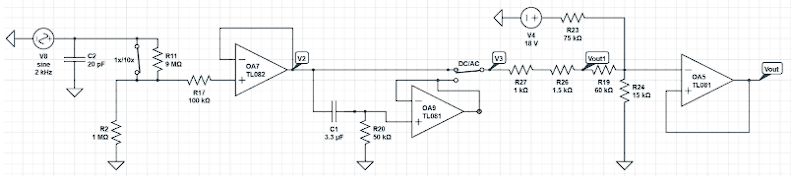
Schematic of the Oscilloscope Input stage, Input Protection Circuit, and Low Pass Filter
Output ADC Circuit and Arduino Nano
Both Copper Layers
Specifically, we modified three areas of our design: 1) Removed R17 (1MΩ) resistor because it may result in a significant offset (because the voltage drop across it due to the non-zero input bias current of the non-ideal op-amp). Also, it adds a lot of noise. 2) Modified the location of the AC/DC switch to be in parallel with the capacitor, to prevent a loading effect from the filter on V2. 3) Used a summing op-amp in the third stage to minimize the loading effect from each input path to the buffer.
For PCB design, we selected Through-Hole as our design pattern, and Connector and Header as our switch connection method.